
It’s a rather old topic and one can find many good references. In this post, I will write down some of my basic understandings on this circuit.
Operation of CML latch
Figure 1 shows a simplified block diagram of divider-by-2 and a CML (current-mode logic) latch. M1/M2 form a preamplifier and M3/M4 a cross-coupled pair. Fig. 2 illustrates the low-frequency and high-frequency operation of CML latch. During the low-frequency operation, when CK is high, the input is amplified by M1/M2; when CK goes low, the cross-coupled pair performs regeneration and latches the state. For short cycle operation, the cross-coupled pair continues to provide gain in the store mode, regenerating to a final differential output of Iss*RL. This condition is met if gm3RL>1.


Speed estimation of CML latch
When CK is high, the circuit can be viewed as a single-pole amplifier. Assume that a step voltage is applied at the input, the differential output voltage can be expressed as

where VXY0 and VXY1 are the initial and final differential output during the sense phase, gm1 is the transconductance of the input transistor, the product of RL and CL is the time constant. RL and CL are the equivalent resistive and capacitive load seeing from node X/Y.
As is shown in Fig.2, in a divider-by-2, input of one latch is output of the other. Both the initial differential voltage at X/Y (VXY0) and the input voltage step (Vstep) have the same value of Iss*RL. Replacing VXY0 and Vstep with Iss*RL, Eq(1) can be rewritten as

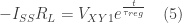
When clock goes low, the latch starts regeneration and the differential output continues to evolve, which can be expressed as

The regenerative time constant equals
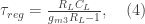
where gm3 is the transconductance of the cross-coupled pair. The latch regenerates the differential output to a final value of -Iss*RL. Replacing VXY2 with -Iss*RL, Eq(3) can be rewritten as
Now we have derived the amplification time, Eq(2), and the regeneration time, Eq(5), respectively. It would be interesting to visualize them in the following plots (Fig.3 and Fig.4). It can be seen that the optimal speed happens when the differential output at the end of the sense phase (VXY1) is between its final settled value and half of it.


The above plots are based on the following assumptions:
- Gm/Id: a value of 10 is a good start. This indicates that operating the transistor in moderate inversion is optimal when we value speed and power efficiency equally. The conversion between Gm/Id and inversion coefficient(IC) can be referred to this post.
- Gain (G): a value around 3 is a good start. For submicron CMOS node, the self-gain of a standard transistor with minimum length is normally no large than 10. In this case, we further assume M1/M2 and M3/M4 have the same size.
- Differential output voltage (Iss*RL): in the range of 400 ~ 600 mV [2].
- Tail current (Iss): assume RL is 500Ohm, Iss around 800uA is a good start point. Then gm = Gm/Id*(Iss/2) = 10*400uA = 4 mA/S. (Note that gmRL > 1 holds)
- Transistor width (W): according to gm/Id simulation of a minimum-length transistor in submicron process, for 1-um width a gm/Id of 10 needs ~150-uA bias current. If the width is 4x, the bias current will be 600uA.
- Capacitive load (CL): the capacitive load contributed by the transistors are equal to 2*Cgg+2*Cdd ~= 3Cgg. With width of 4um and length of 30nm, the Cgg can be approximated to about 2.4fF (4*0.03*20=2.4fF). Normally, the load from a succeeding buffer will dominate.
The Matlab script used to plot the data can be found here.
References:
[1] Online lecture notes (Access Jan.05, 2021), https://people.engr.tamu.edu/spalermo/ecen620/lecture12_ee620_dividers.pdf
[2] B. Razavi, “The Cross-Coupled Pair – Part II [A Circuit for All Seasons],” IEEE Solid-State Circuits Magazine, Issue 4, pp. 9-12, Fall 2014.

Pingback: [M scripts] Speed estimation of CML latch | EveryNano Counts
🐂